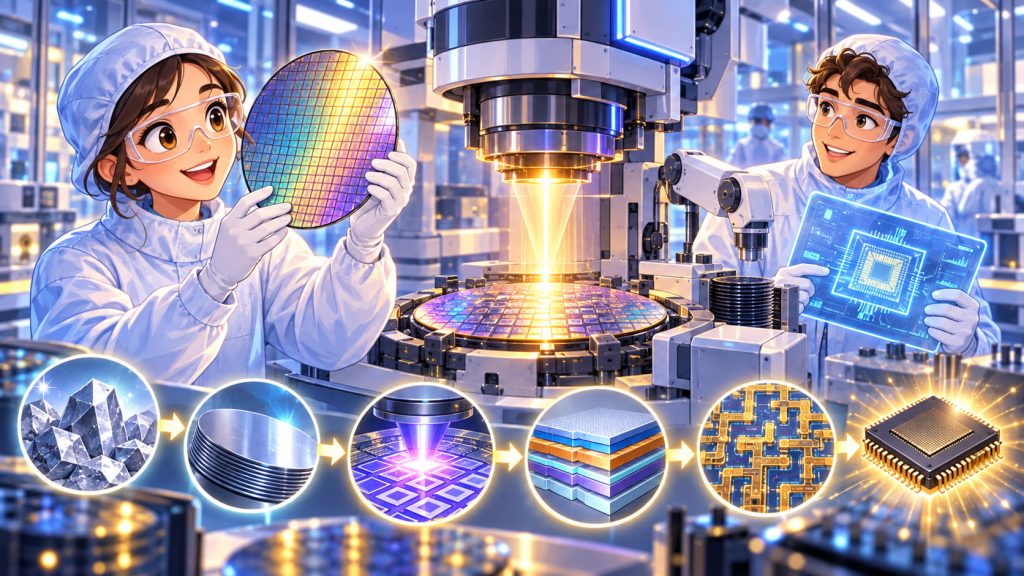
Computer chips power almost everything in modern life. Smartphones, cars, laptops, satellites, medical equipment, game consoles, data centers, and even household appliances depend on tiny pieces of silicon packed with extraordinary complexity.
A modern processor may contain billions of transistors, each so small that thousands can fit across the width of a human hair.
Yet chips do not begin as miniature computers. Their creation starts with extremely pure materials, advanced physics, precise chemistry, and factories so clean that even microscopic dust can ruin production.
Here is how computer chips are made, step by step.
It Starts With Silicon
Most computer chips are built primarily from silicon, one of the most abundant elements in Earth’s crust.
Silicon is commonly found in minerals such as quartz and silica. The raw material must be purified to an extraordinarily high level before it can be used in electronics.
The purified silicon is melted and formed into a large single crystal.
One common method slowly pulls a seed crystal from molten silicon while rotating it. The result is a cylindrical crystal called an ingot.
This crystal can be hundreds of millimeters in diameter.
Turning a Silicon Crystal Into Wafers
The silicon ingot is sliced into extremely thin circular discs called wafers.
These wafers become the foundation on which hundreds or thousands of individual chips are manufactured simultaneously.
The wafer surfaces must be almost perfectly flat.
They are ground, polished, and cleaned until microscopic imperfections are minimized.
Modern high-volume semiconductor manufacturing commonly uses wafers around 300 millimeters in diameter.
A single wafer can eventually contain hundreds of finished processor dies, depending on chip size.
The Chip Is Designed Before It Is Manufactured
Long before a wafer enters a factory, engineers design the chip digitally.
Modern chips can require years of development.
Designers create circuits containing processors, memory systems, communication interfaces, power-management components, and billions of interconnected transistors.
Specialized software known as electronic design automation, or EDA, helps engineers convert circuit designs into physical layouts.
The final design is broken into many layers.
Each layer determines where specific structures will be created on the silicon wafer.
Photolithography: Printing Microscopic Patterns
One of the most important processes in chip manufacturing is photolithography.
The wafer is coated with a light-sensitive chemical material called photoresist.
Light is then projected through or reflected from a specially prepared pattern called a mask.
The light changes selected regions of the photoresist.
After chemical processing, parts of the coating are removed, leaving a microscopic pattern on the wafer.
This pattern becomes a guide for later manufacturing steps.
The basic idea resembles photography or printing, but the scale is extraordinarily small.
Extreme Ultraviolet Lithography
The most advanced chips require features only a few nanometers across.
Creating patterns at this scale requires extremely sophisticated technology.
Modern leading-edge factories use extreme ultraviolet lithography, or EUV.
EUV systems use light with a wavelength of approximately 13.5 nanometers.
Producing and controlling this light is extremely difficult.
Inside an EUV machine, powerful lasers strike tiny droplets of molten tin, generating plasma that emits extreme ultraviolet radiation.
Special mirrors then guide and focus the light onto the wafer.
These machines are among the most complex manufacturing systems ever built.
Building Transistors Layer by Layer
A transistor is essentially a microscopic electronic switch.
Modern processors contain billions of them.
To manufacture transistors, chipmakers repeatedly add, remove, and modify extremely thin layers of material.
Important processes include:
- Deposition
- Etching
- Ion implantation
- Oxidation
- Lithography
- Cleaning
- Chemical-mechanical polishing
These steps may be repeated hundreds or even thousands of times during production.
A modern chip is not simply printed once. It is constructed layer by layer through an enormous sequence of highly controlled processes.
Deposition Adds Thin Materials
During deposition, extremely thin layers of material are placed onto the wafer.
These layers may consist of insulators, conductors, or semiconductor materials.
Some layers can be only a few atoms thick.
Techniques such as chemical vapor deposition and atomic layer deposition allow engineers to control thickness with extraordinary precision.
Different materials perform different roles in the finished chip.
Some carry electrical current, while others isolate nearby structures.
Etching Removes Material
After lithography creates a pattern, unwanted material must often be removed.
This is called etching.
Chemical or plasma-based processes can selectively remove exposed material while leaving protected areas intact.
Advanced plasma etching allows manufacturers to create incredibly narrow and deep structures.
The process must be carefully controlled because removing even slightly too much material can change transistor performance.
Doping Changes Silicon’s Electrical Behavior
Pure silicon is not enough to create useful electronic circuits.
Its electrical properties must be modified.
This is done through doping, where carefully selected atoms are introduced into the silicon.
One method uses ion implantation.
Charged atoms are accelerated toward the wafer and embedded into specific regions.
Different dopants create areas with different electrical characteristics.
These regions become essential parts of transistors and other semiconductor devices.
Connecting Billions of Transistors
Creating the transistors is only part of the job.
They must also be connected together.
Manufacturers build multiple layers of microscopic metal wiring above the transistors.
These interconnects carry electrical signals across the chip.
Modern processors can contain many metal layers stacked vertically.
Tiny vertical connections called vias link one layer to another.
The result is an incredibly dense three-dimensional network of electronic pathways.
Why Chip Factories Are So Clean
Semiconductor factories are known as fabs.
Some parts of these facilities operate as advanced cleanrooms.
Tiny dust particles that would be invisible to the human eye can be enormous compared with modern transistor features.
A particle landing on the wrong part of a wafer could destroy multiple circuits.
Air is therefore continuously filtered, while temperature, humidity, vibration, and contamination are tightly controlled.
Workers wear specialized cleanroom clothing designed to prevent skin particles, hair, and other contaminants from reaching the production environment.
Testing Every Chip
Not every chip manufactured on a wafer works perfectly.
After fabrication, automated equipment tests individual dies while they are still attached to the wafer.
Defective dies are identified and excluded.
The percentage of usable chips produced from a wafer is known as yield.
High yield is extremely important economically.
If too many chips are defective, manufacturing becomes much more expensive.
Expert Perspective: Manufacturing Precision Matters as Much as Design
Semiconductor industry experts have long emphasized that designing an advanced chip is only half the challenge.
TSMC founder Morris Chang has repeatedly highlighted the importance of manufacturing capability and operational excellence in the semiconductor industry.
A brilliant processor architecture has little commercial value if factories cannot manufacture it reliably in enormous quantities.
Modern chip production is therefore a combination of physics, engineering, chemistry, software, and extraordinarily disciplined manufacturing.
Cutting the Wafer Into Individual Chips
Once testing is complete, the wafer is cut apart.
This process is called dicing.
Each small rectangular piece is known as a die.
A die contains the actual electronic circuitry of the chip.
Good dies are selected for packaging.
Packaging Protects and Connects the Chip
Bare silicon dies are extremely fragile and difficult to connect directly to a circuit board.
Packaging protects the die and provides electrical connections to the outside world.
Modern packaging can be surprisingly sophisticated.
Some processors combine multiple smaller dies called chiplets inside a single package.
Advanced packages may also place logic chips close to high-speed memory.
This allows manufacturers to build powerful systems without creating every component on one enormous piece of silicon.
Why Chip Manufacturing Takes So Long
A wafer may travel through a semiconductor factory for weeks or months.
During that time, it moves repeatedly between lithography tools, deposition chambers, etching machines, cleaning stations, inspection systems, and measurement equipment.
Every layer must align precisely with the previous layers.
Even tiny errors can make a chip unusable.
Producing advanced semiconductors therefore requires some of the most precise manufacturing processes humans have ever developed.
Interesting Facts
- A modern high-performance processor can contain tens of billions of transistors.
- Silicon wafers used in advanced semiconductor factories are commonly about 300 millimeters across.
- Some layers deposited during chip manufacturing can be only a few atoms thick.
- EUV lithography uses light with a wavelength of roughly 13.5 nanometers.
- Advanced chips may require hundreds of separate manufacturing steps.
- Semiconductor cleanrooms contain dramatically fewer airborne particles than ordinary indoor environments.
- A single wafer may contain hundreds of individual chip dies.
- Chip manufacturing requires ultrapure water in enormous quantities for cleaning wafers.
- Modern processors can contain many layers of microscopic metal wiring.
- Advanced semiconductor factories can cost tens of billions of dollars to build.
- Chiplets allow several smaller pieces of silicon to work together as one larger processor.
Glossary
- Semiconductor — A material whose electrical conductivity can be controlled, making it useful for electronic devices.
- Silicon — The primary semiconductor material used in most modern computer chips.
- Wafer — A thin circular slice of semiconductor material on which chips are manufactured.
- Transistor — A microscopic electronic component that can switch or control electrical signals.
- Die — An individual piece of a semiconductor wafer containing one complete chip circuit.
- Photolithography — A manufacturing technique that uses light to transfer microscopic patterns onto a wafer.
- EUV Lithography — Extreme ultraviolet lithography, an advanced method used to create extremely small features on modern chips.
- Photoresist — A light-sensitive chemical coating applied to wafers during lithography.
- Etching — The controlled removal of material from selected areas of a wafer.
- Deposition — The process of adding extremely thin layers of material to a wafer.
- Doping — The introduction of specific atoms into a semiconductor to change its electrical properties.
- Ion Implantation — A technique that embeds charged atoms into semiconductor material.
- Interconnect — Microscopic metal wiring connecting transistors and other components inside a chip.
- Via — A tiny vertical electrical connection between different wiring layers.
- Fab — A semiconductor fabrication facility where computer chips are manufactured.
- Yield — The percentage of manufactured chips that function correctly.
- Dicing — The process of cutting a completed wafer into individual dies.
- Chiplet — A small specialized semiconductor die designed to operate together with other dies inside one package.